Critical components. Precisely Tested.
Our methods combine high-end laboratory technology with years of hands-on experience. This ensures precise, reproducible results and full traceability.
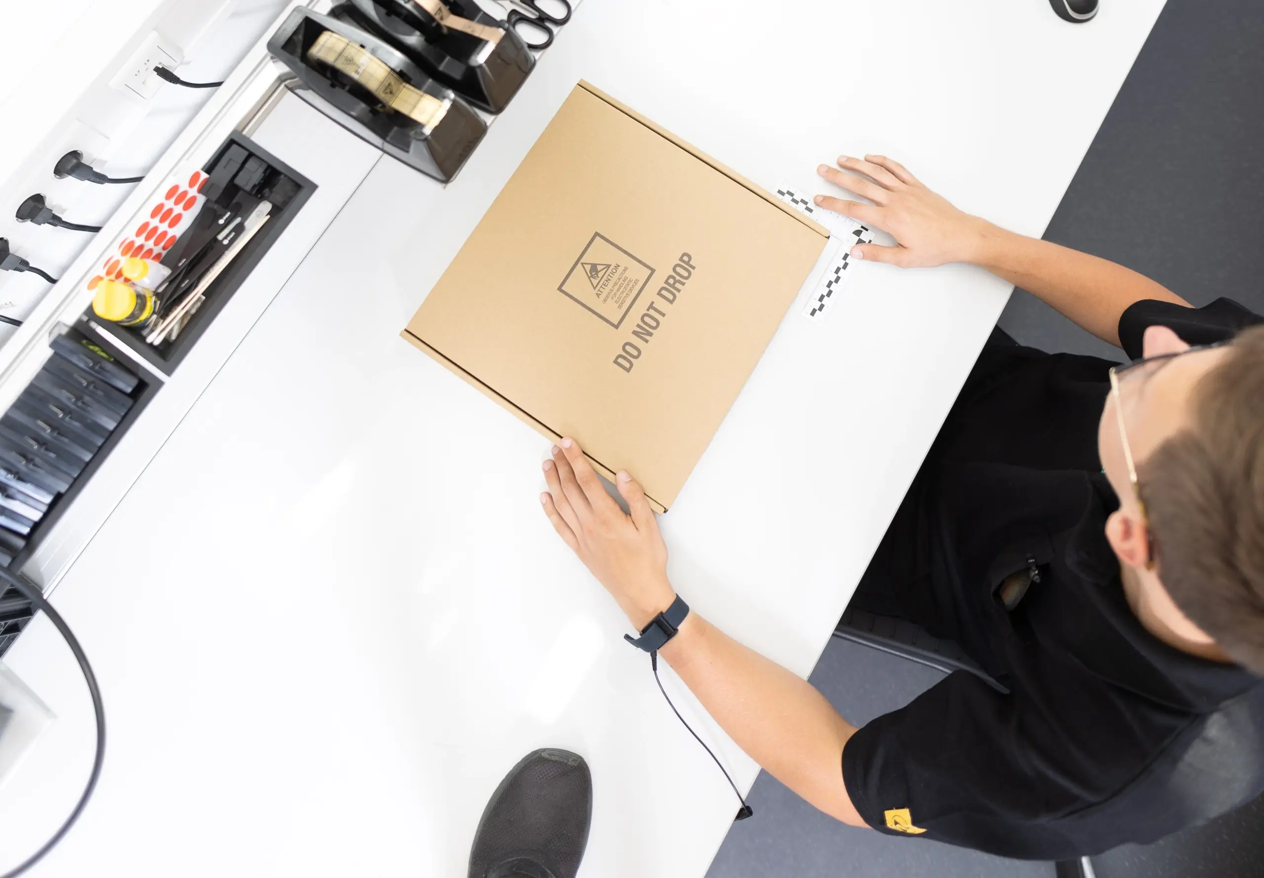
1. Incoming Inspection
Our incoming inspection begins with a check of the shipping packaging for transport damage. Then, we verify the delivery note, labeling, and packaging details using an AI-assisted benchtop scanner. This scanner captures all label information in detail and compares it against the order data.
Next, we conduct a fast yet highly precise X-ray inspection to confirm the delivered quantity—providing exact results in just seconds.
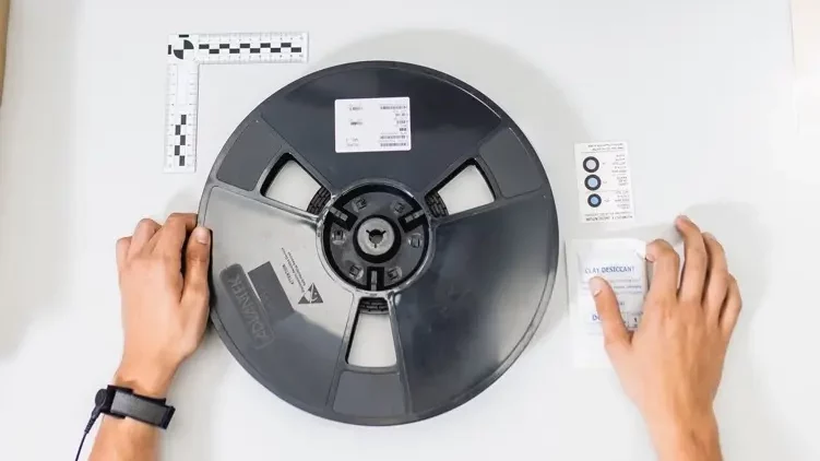
The analysis continues: We examine packaging authenticity using high-resolution digital cameras. Here, our team’s extensive experience plays a key role, especially when evaluating logos and labels. We also inspect for ESD and moisture protection. Trays and tape reels are checked for damage or insufficient leader sections and are supplemented if necessary.
In total, components may undergo up to 25 individual inspection steps—ensuring a complete and reliable incoming quality analysis.
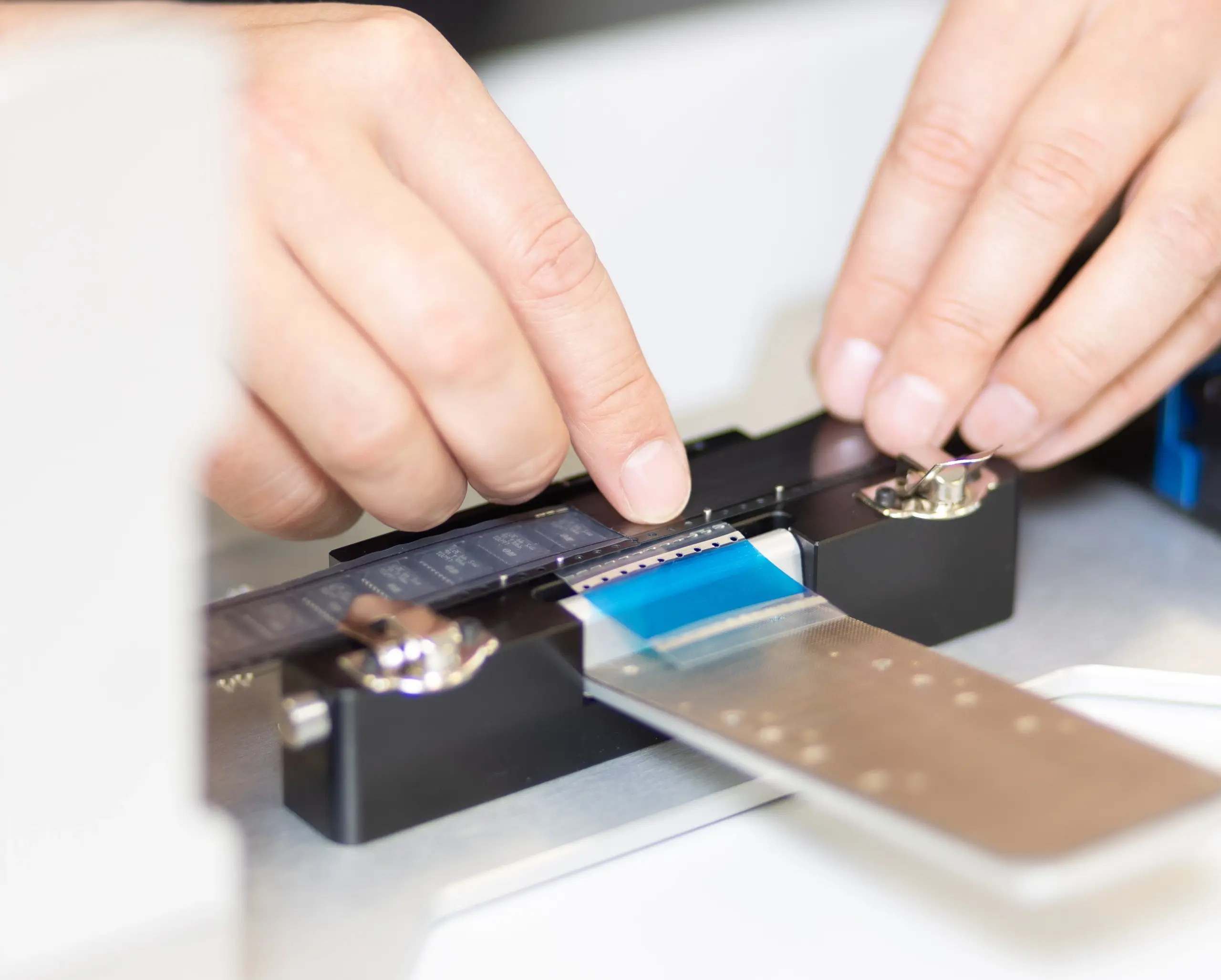
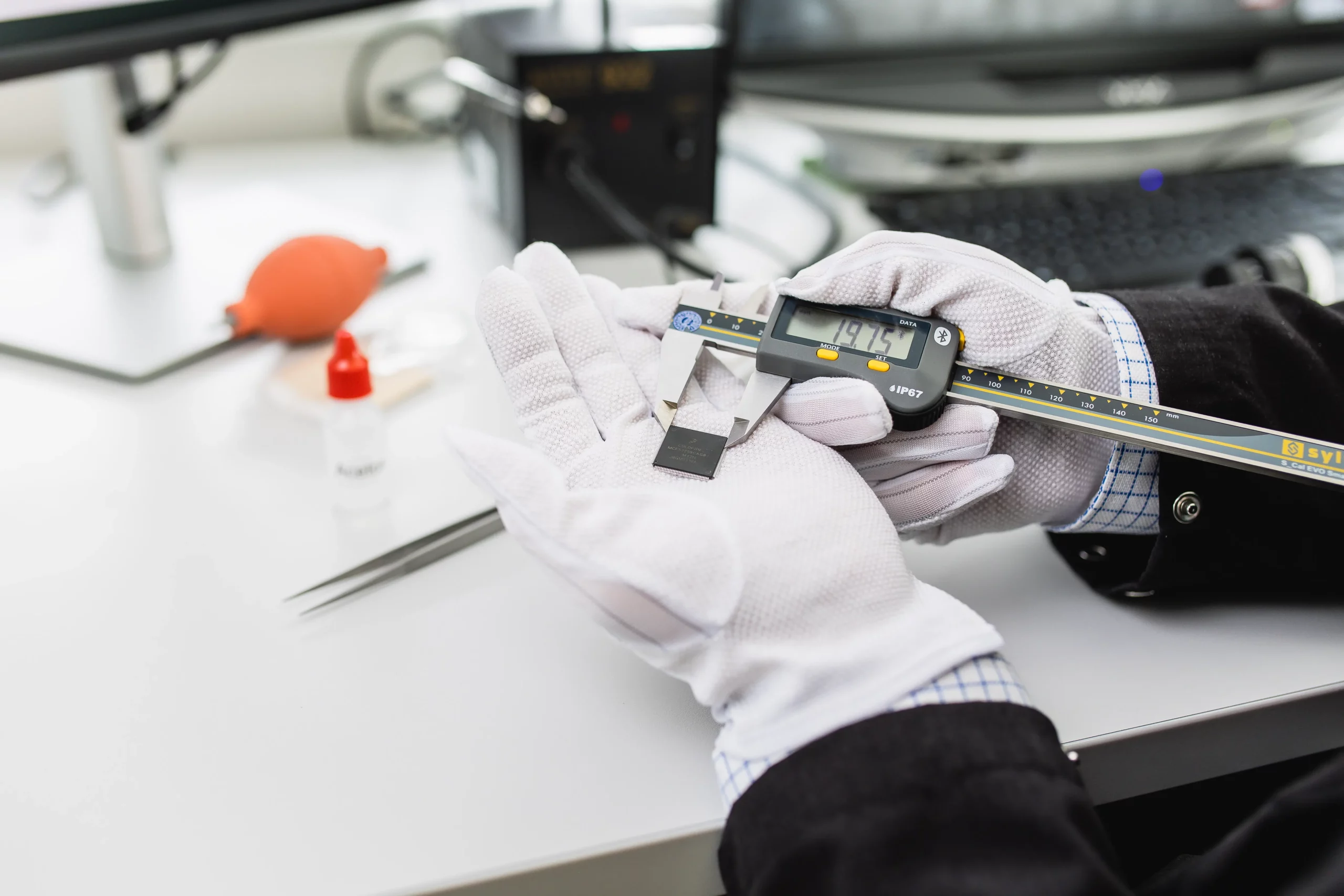
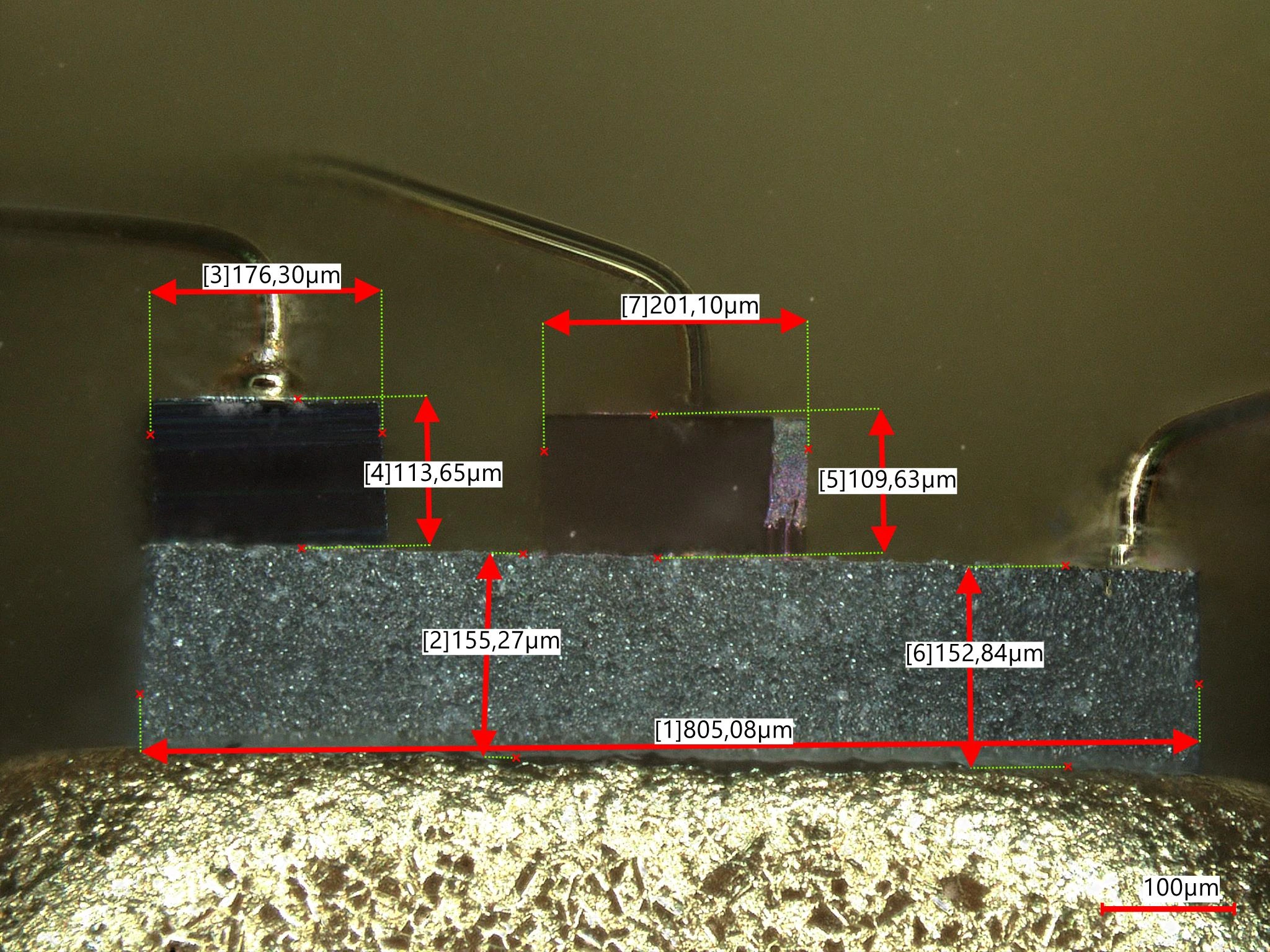
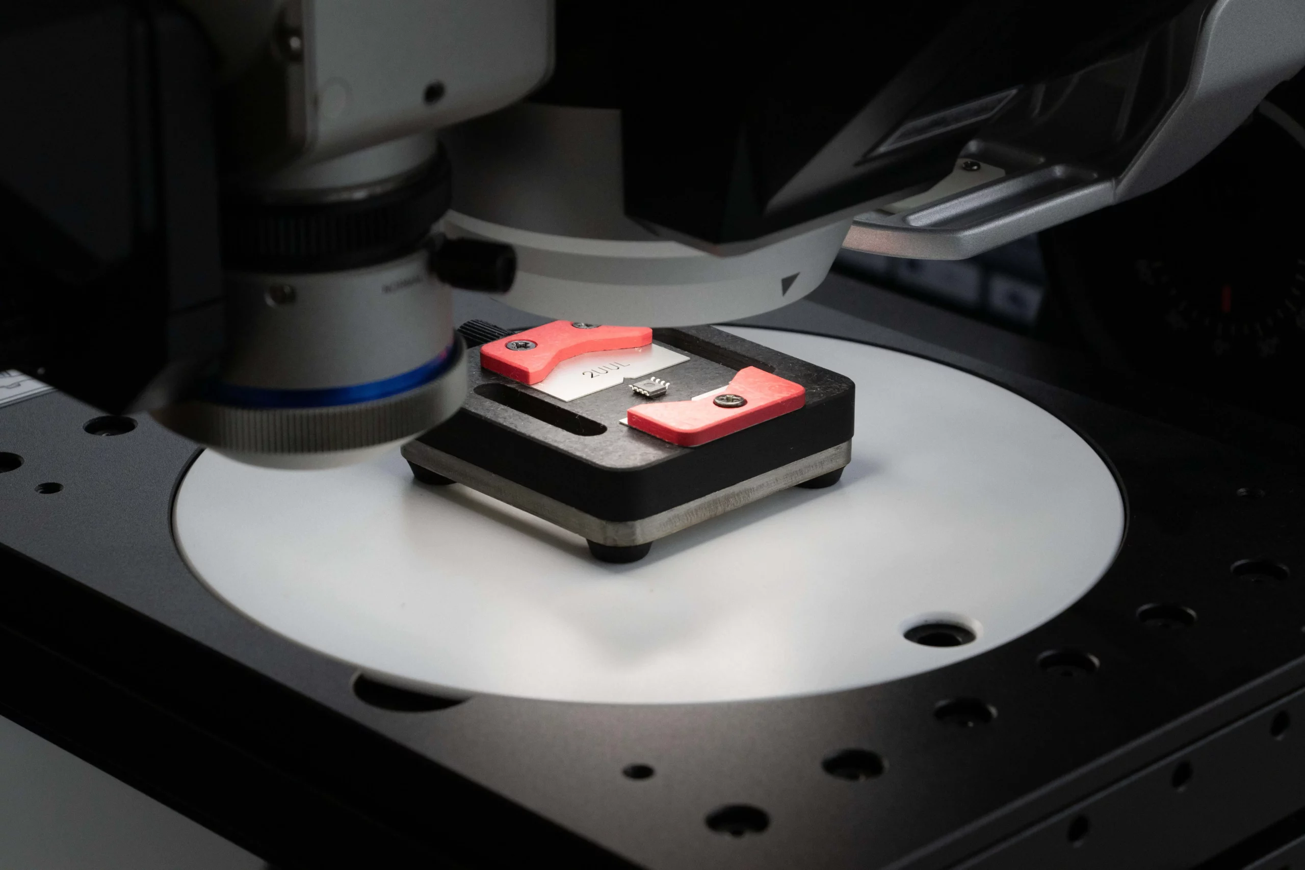
2. Dimensional Measurement
To verify the authenticity and accuracy of electronic components, we systematically measure their geometric properties using high-precision metrology equipment. This includes length, width, height, pin spacing, and other critical dimensions.
These measurements reliably rule out mix-ups or tampering, and they are especially valuable for custom components manufactured according to customer specifications, ensuring exact compliance with design requirements.
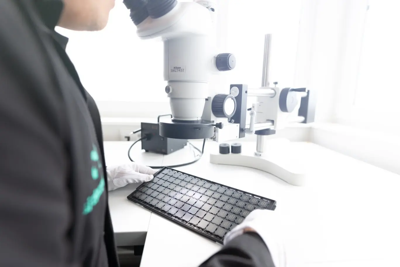
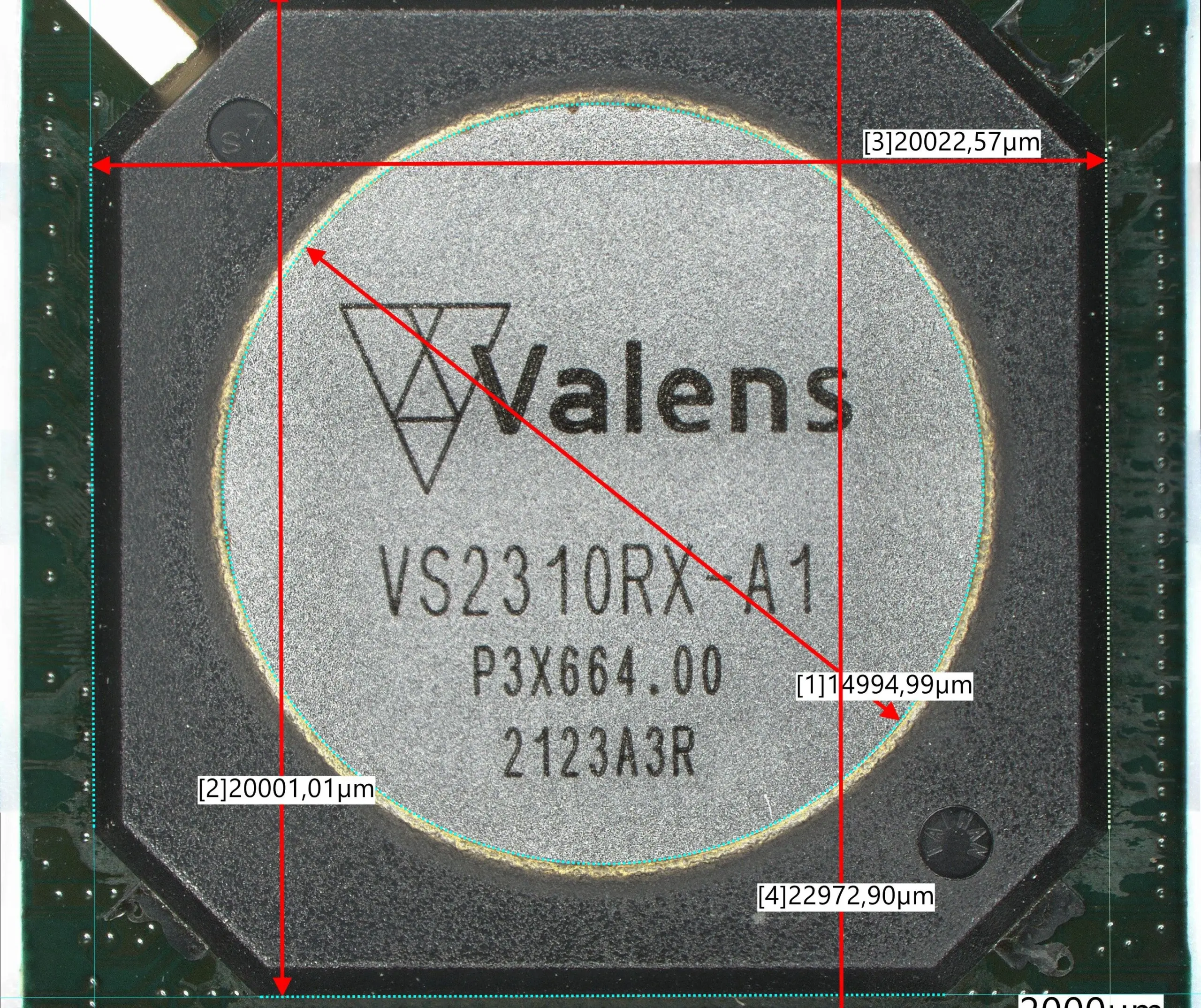
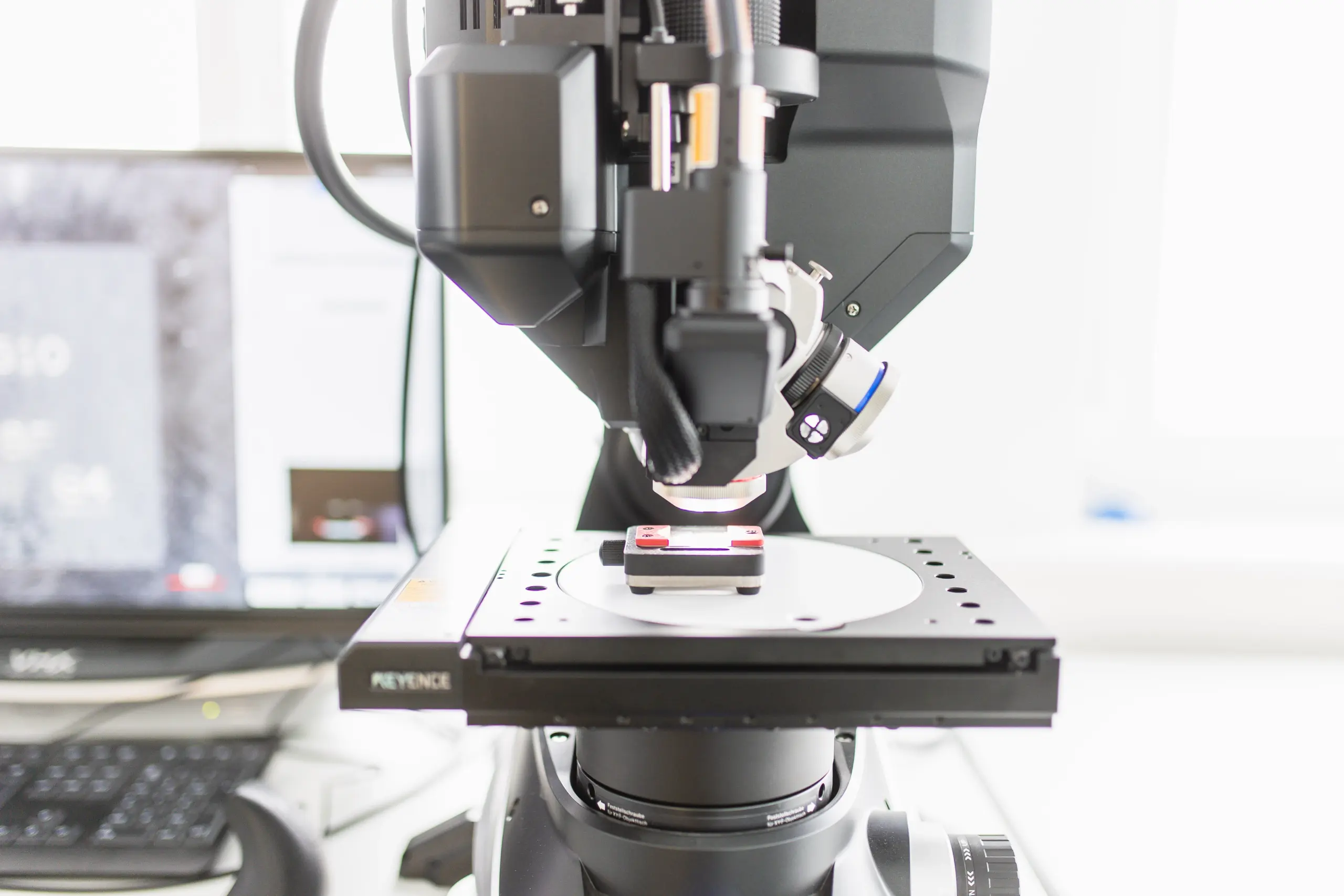
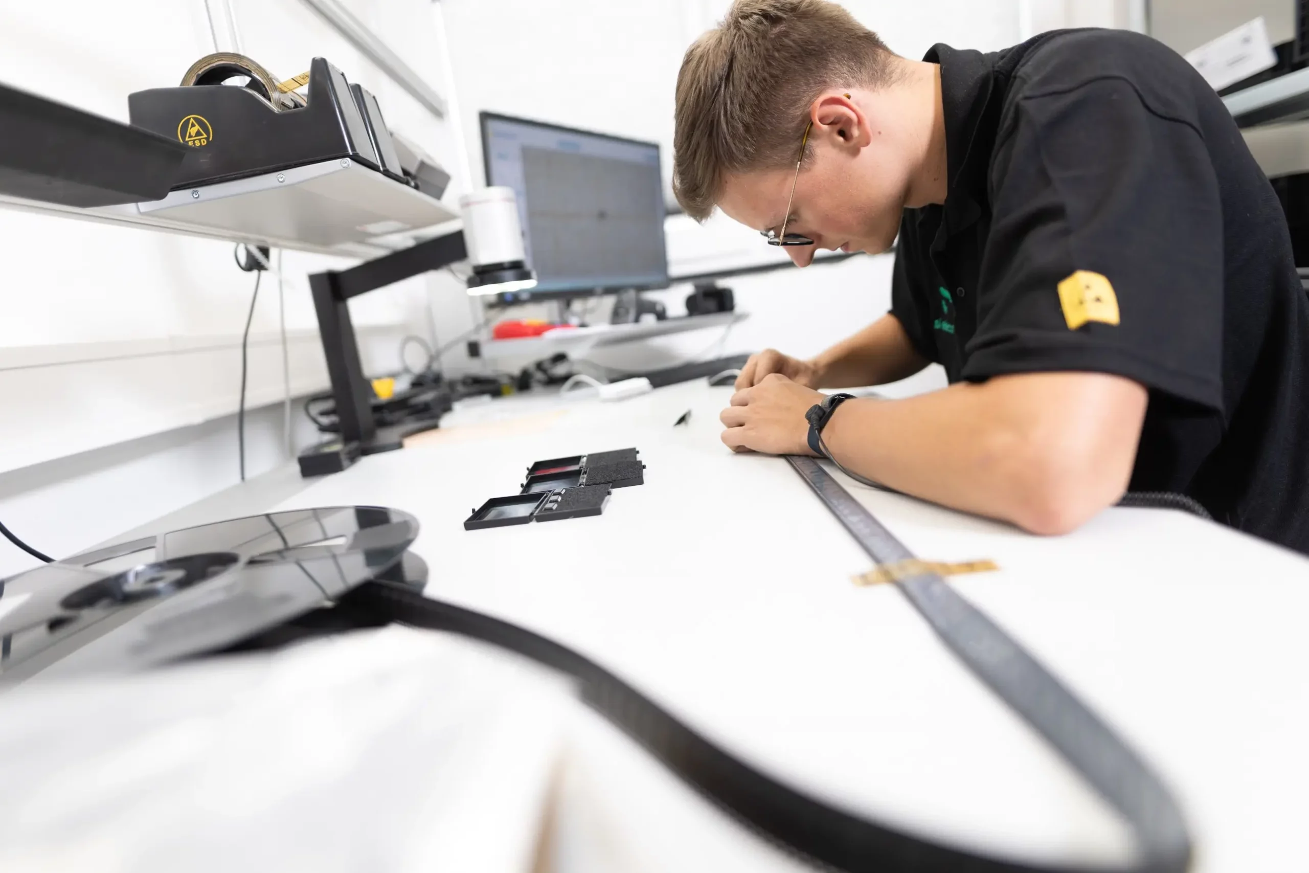
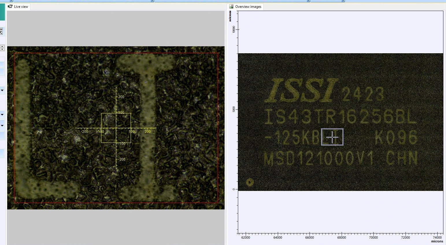
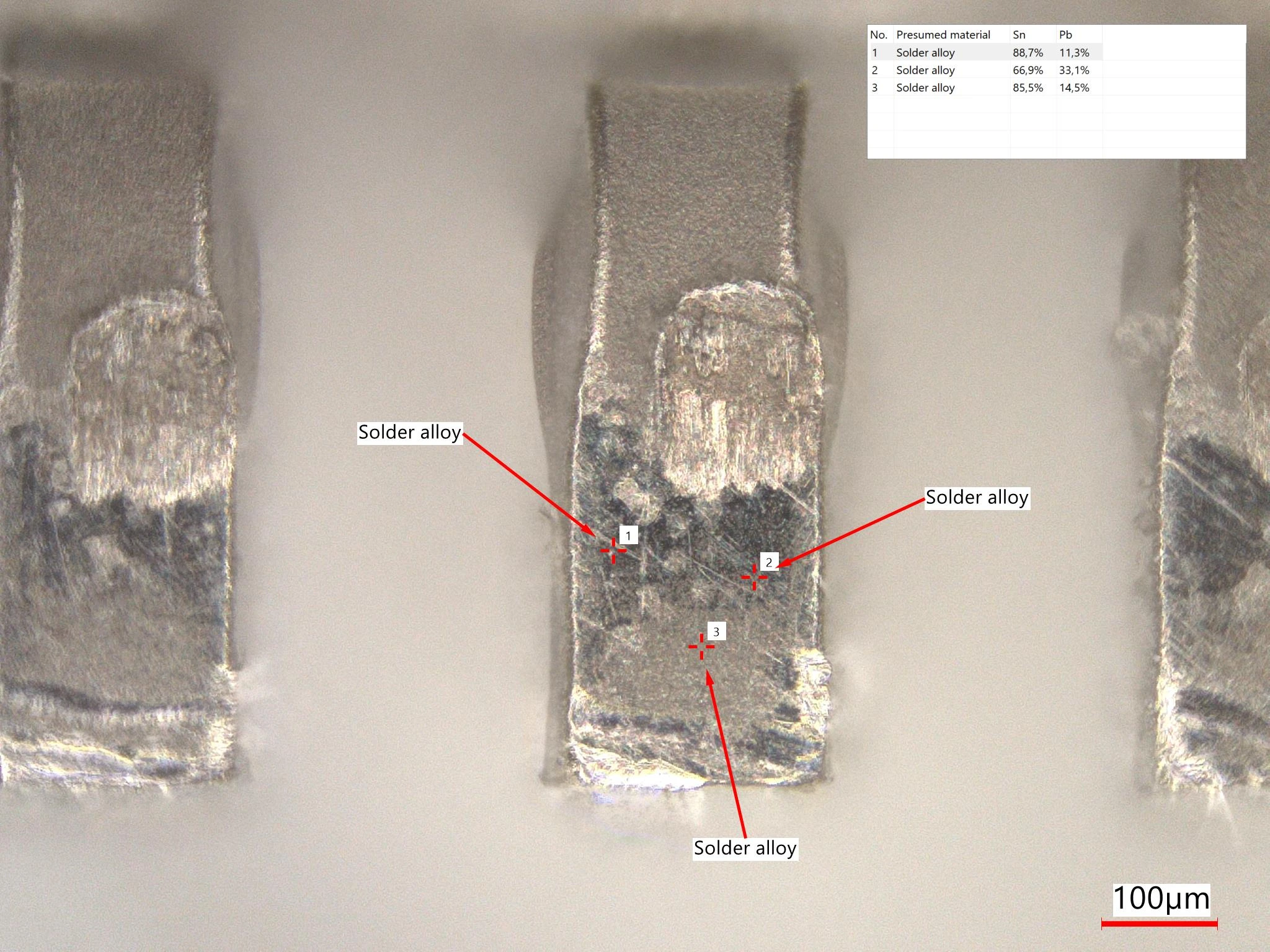
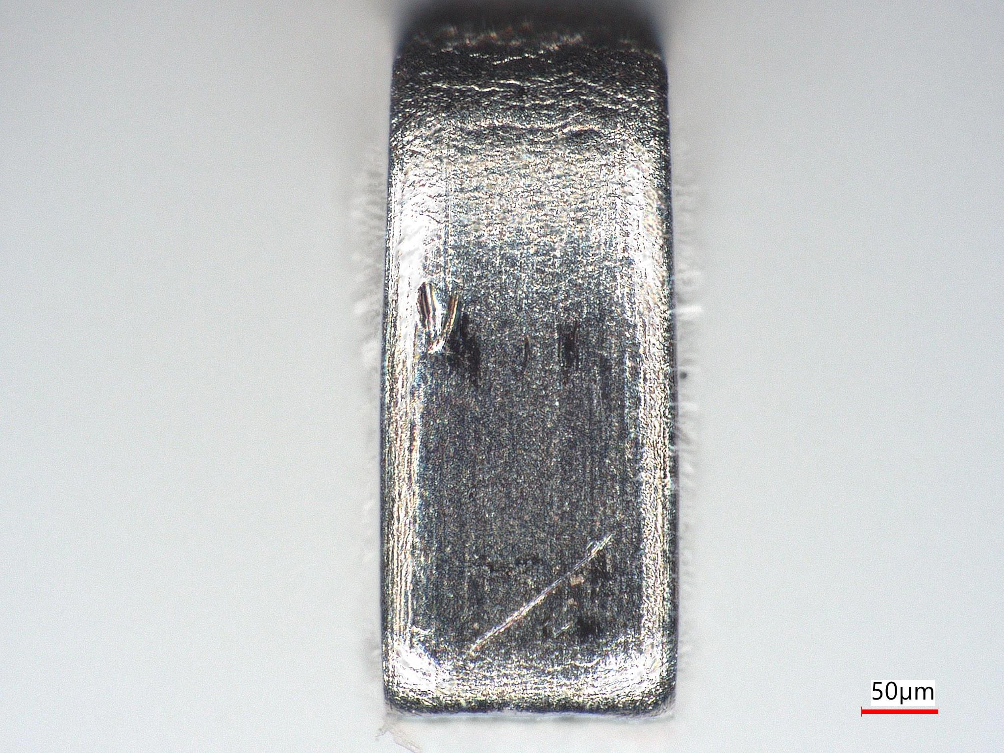
3. Microscopy
Optical microscopy is one of the most essential techniques in quality assessment. A broad range of magnifications and lighting methods allows for the visualization of diverse structural features. With resolutions down to 1 µm, even the slightest signs of improper handling or tampering can be detected.
The images captured during this process are analyzed and interpreted by our experienced team members, specializing in semiconductor technology, polymer science, and materials engineering. They examine the surface structure of encapsulation materials, inspect solder joints for microscopic damage, corrosion, and oxidation, and verify the plausibility of the date code.
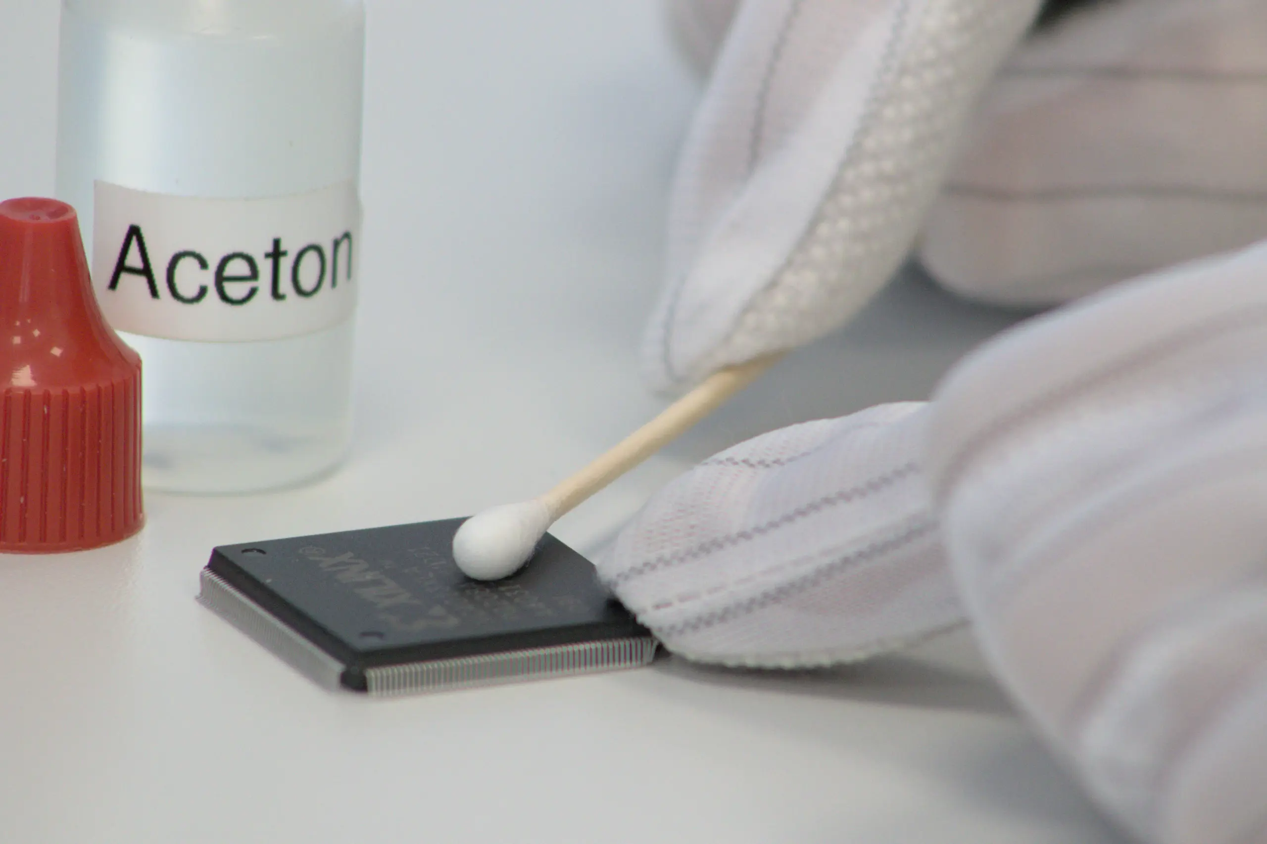
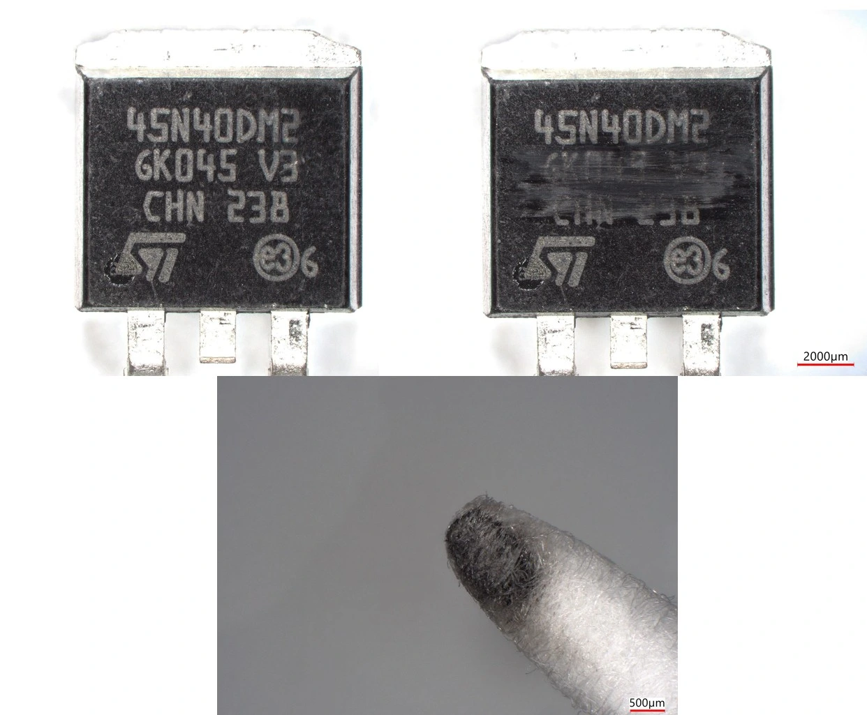
4. Acetone Surface Test
We inspect component surfaces specifically for post-processing coatings (“blacktopping”) and other forms of tampering. Using an acetone test, we reliably detect overpainted markings and concealed refurbishment attempts.
This method is complemented by visual inspection and, if necessary, an additional scrape test to reveal subtle manipulations when acetone results are inconclusive. These findings help you identify hidden risks early and confidently rule out counterfeits.
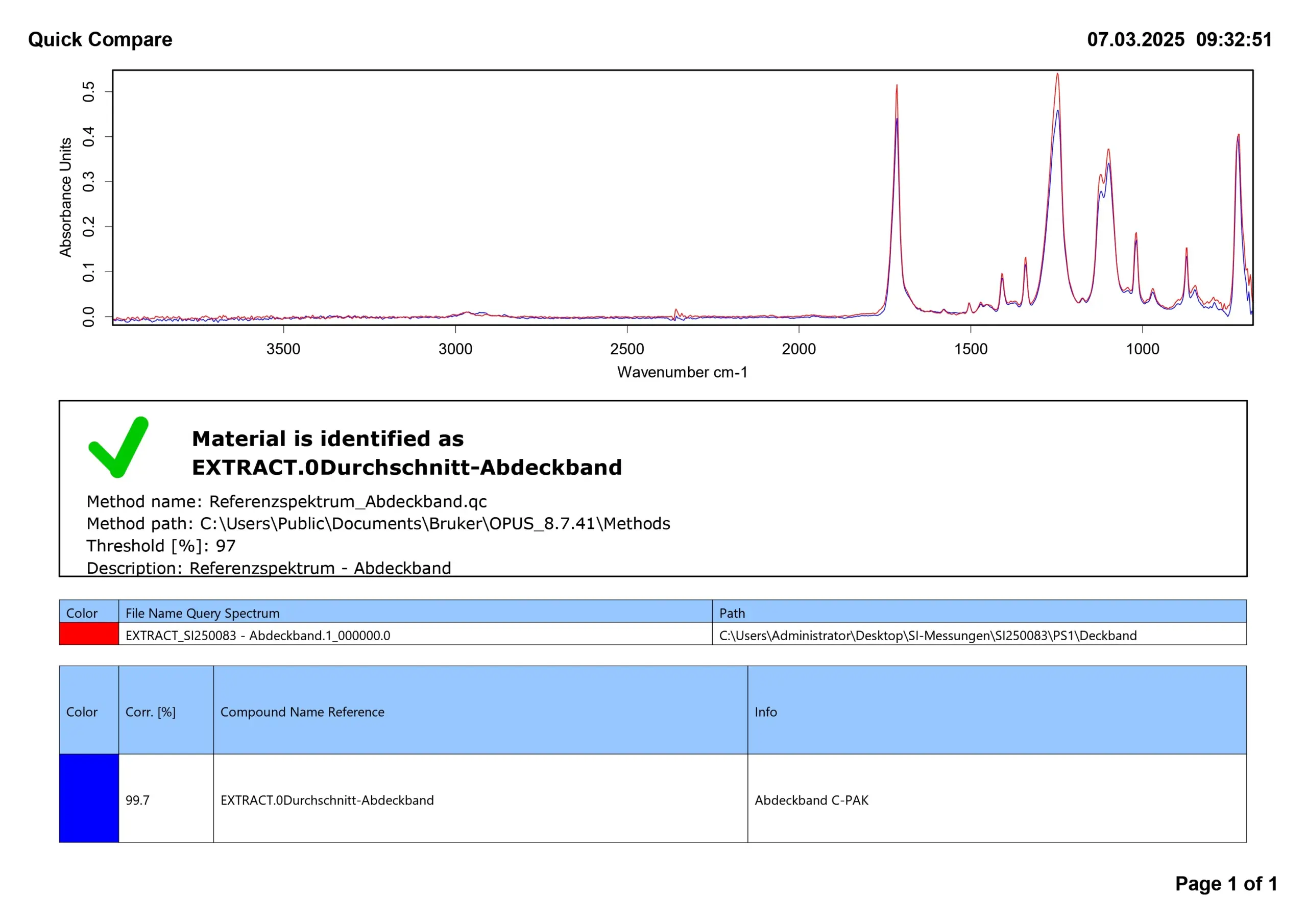
5. FTIR Analysis
FTIR (Fourier-transform infrared) spectroscopy is a non-destructive method that significantly enhances our testing capabilities by enabling the identification of organic and inorganic substances. By analyzing a material’s characteristic infrared spectrum, we can precisely determine its composition.
Typical applications include detecting impurities, additives, contamination, and signs of aging. FTIR analysis provides clear answers to questions such as:
“Is this the same plastic as in the reference sample?”
“What type of contamination is causing adhesion problems?”
“Has the surface been altered or manipulated?”
By comparing spectral data to reference libraries, we can accurately identify materials. FTIR is also highly compatible with optical microscopy, enabling deeper, more contextual and detailed interpretation.
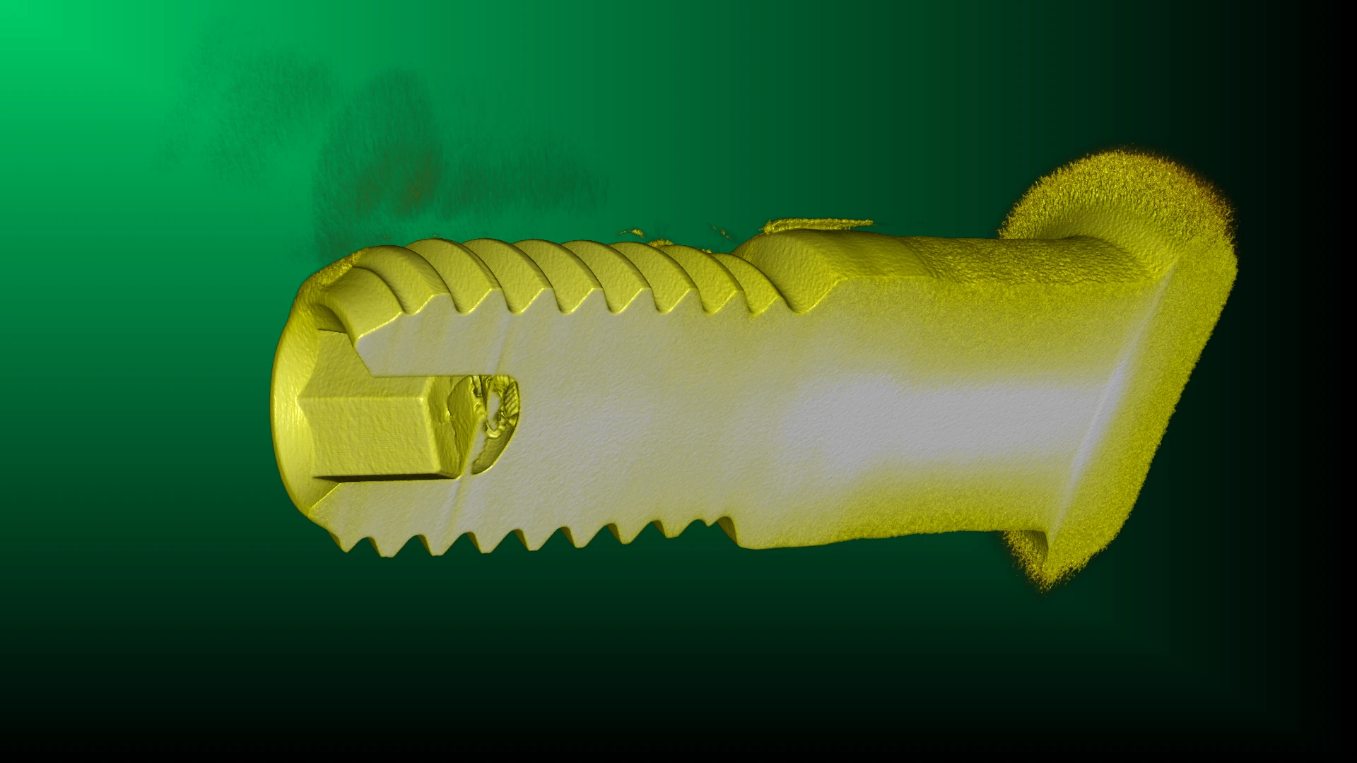
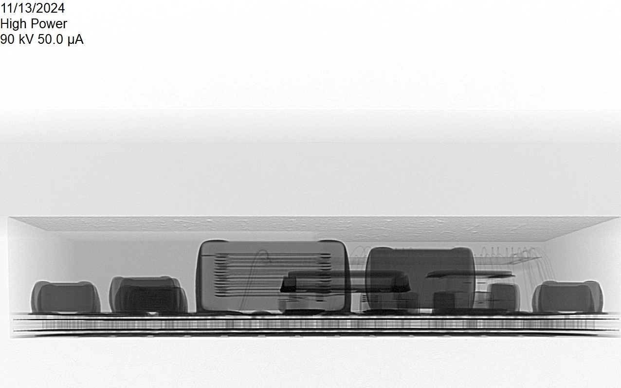
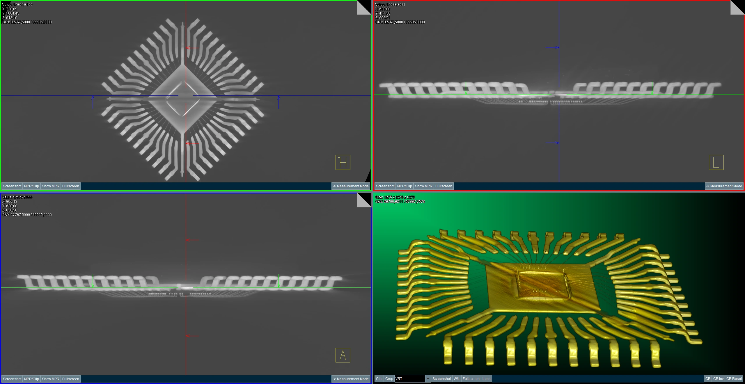
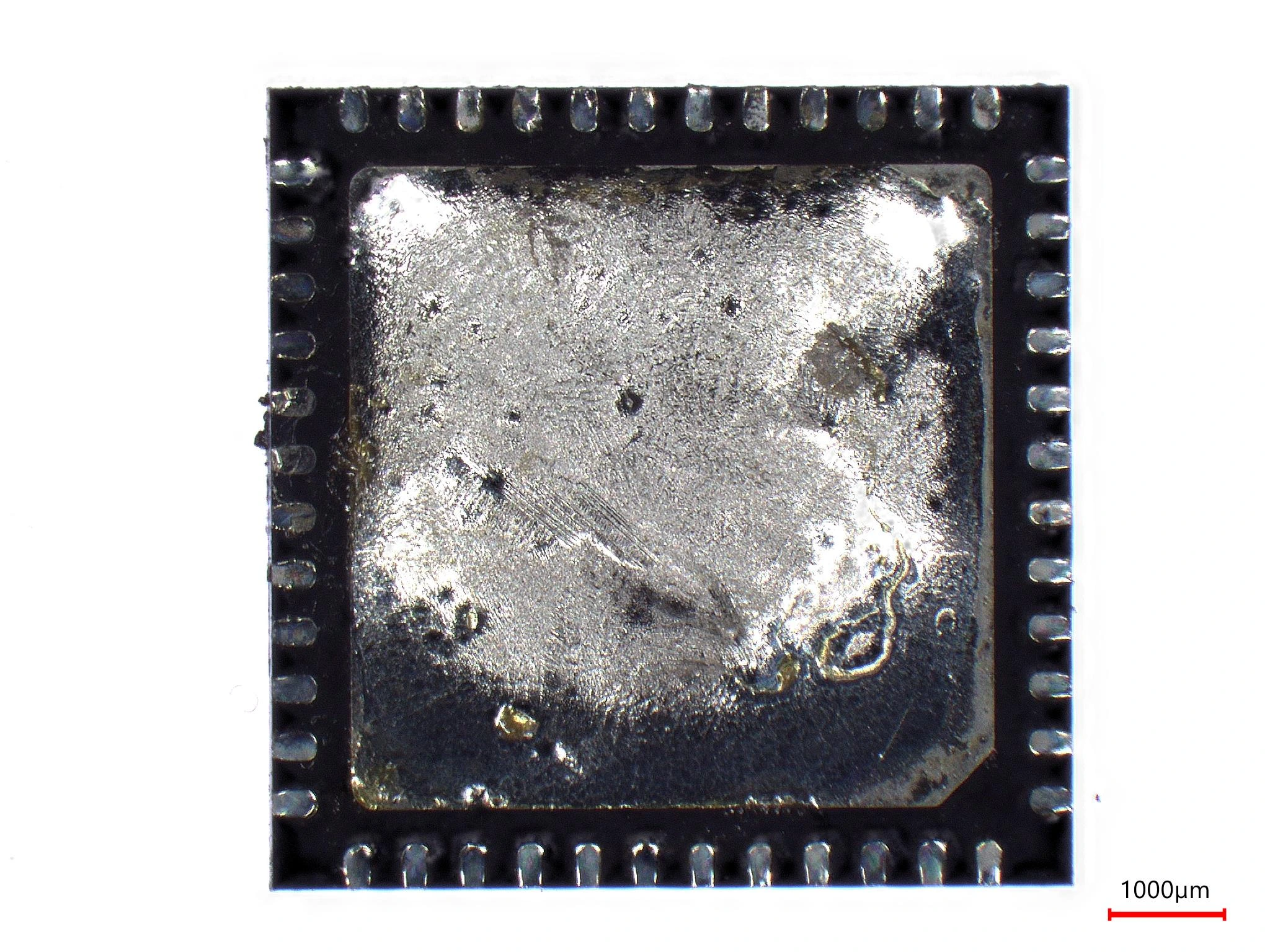
6. X-Ray Inspection
At the SI TechLAB, we use advanced, high-resolution X-ray technology, including 2D imaging, CT, and laminography, to examine the internal structures of components non-destructively. Our six-axis system enables comprehensive analysis of complex geometries and assemblies.
We detect dummy components, bonding defects, missing structures, and internal inconsistencies. Comparative analysis with reference samples (“golden samples”) allows us to reliably identify cloned parts or mixed lots without damaging the components.
This technology also enables full 3D imaging of internal structures, significantly increasing the depth of information. Even the smallest areas of assemblies can be visualized, including traces of flux residue beneath components.
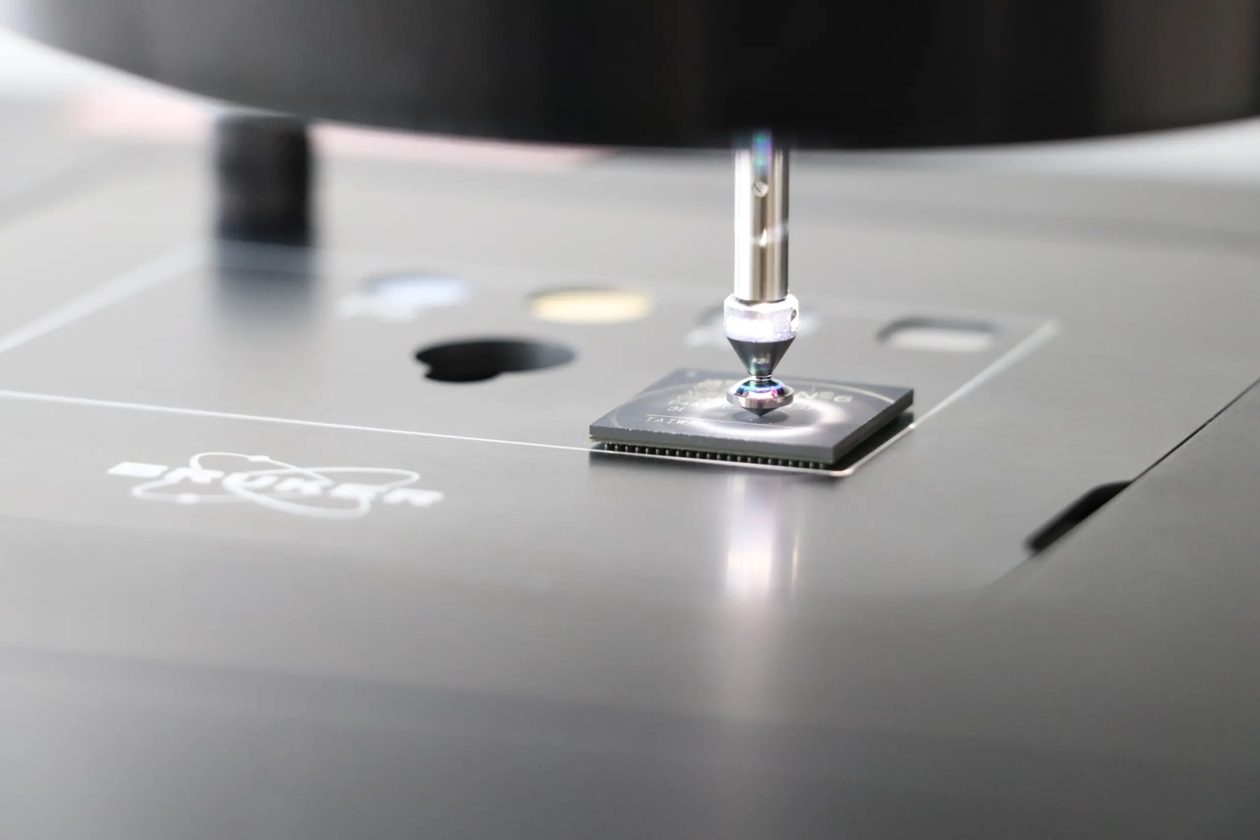
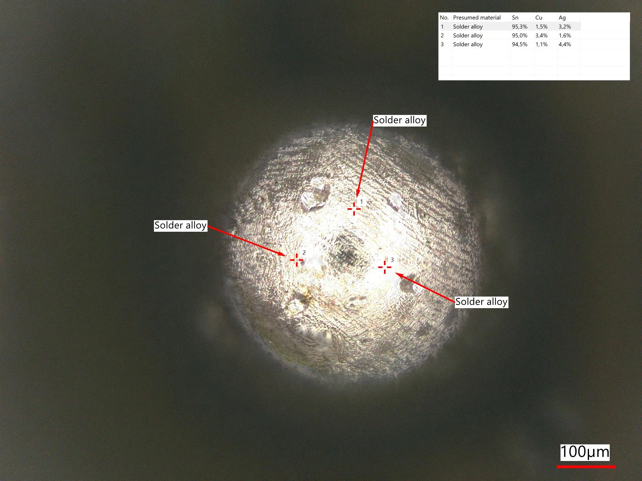
7. Material Analysis (LIBS)
Laser-induced breakdown spectroscopy (LIBS) is an analytical technique used to determine the chemical composition of materials. It works by directing a high-energy laser pulse at the material’s surface to generate a plasma plume. As the plasma cools and transitions phases, excited atoms and ions emit light in the form of emission spectra, each uniquely characteristic of the elements present.
By analyzing this light, LIBS can identify and quantify the elemental composition of a sample. At the SI TechLAB, the LIBS spectrometer is integrated into a microscope system, enabling extremely fast analysis—even of very small areas.
This method is primarily used to analyze surface coatings, such as solder materials, or to detect surface contamination.
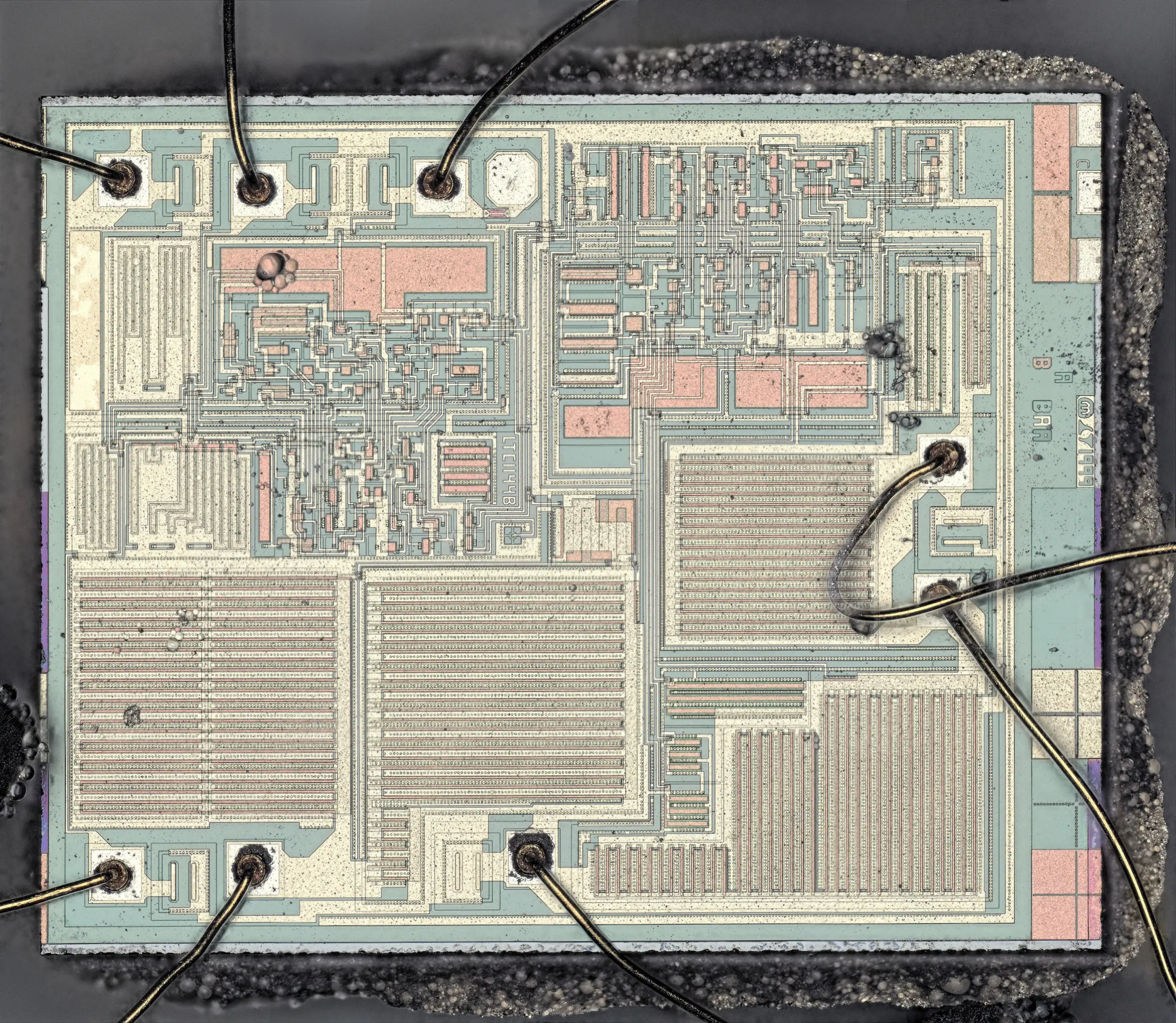
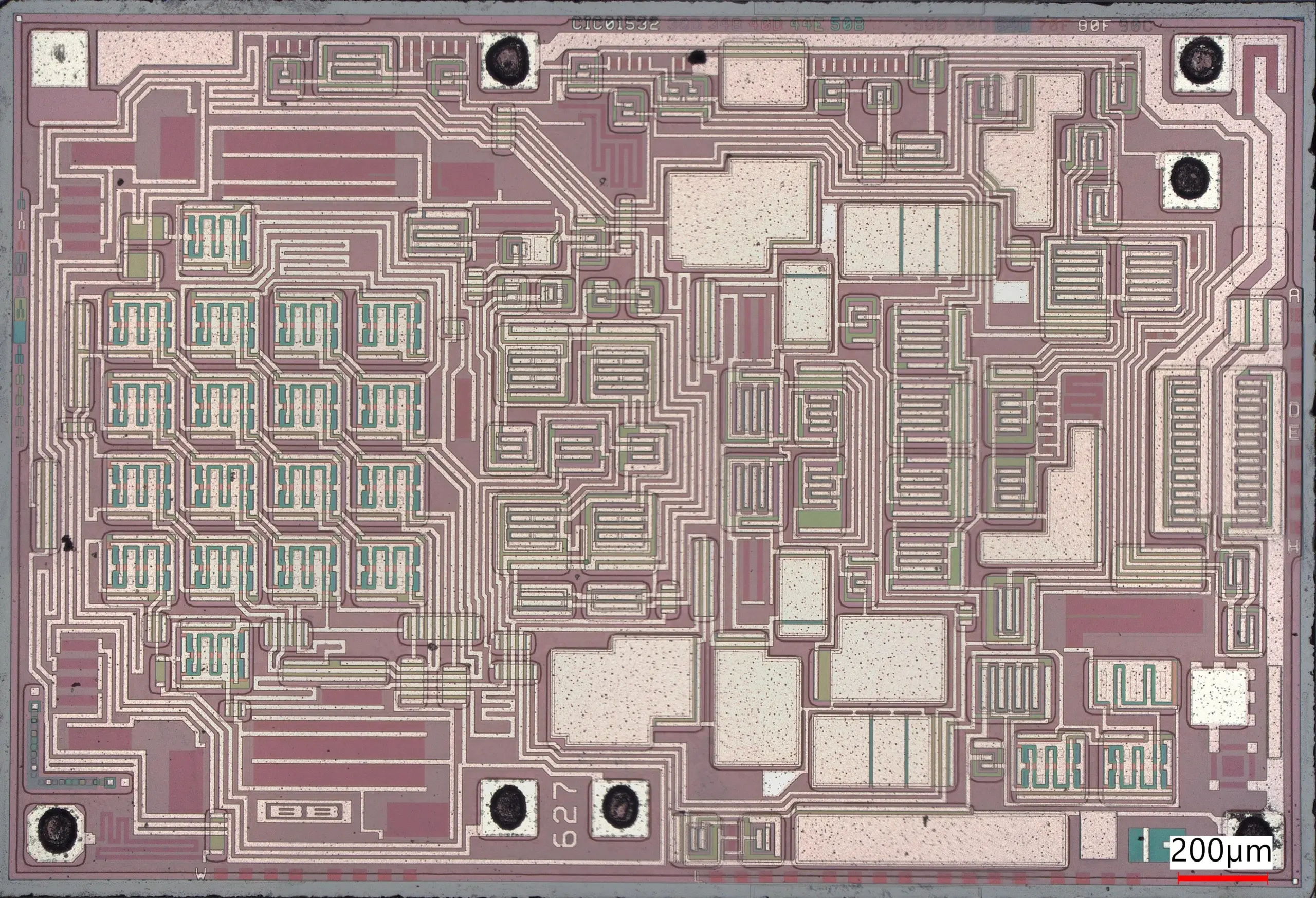
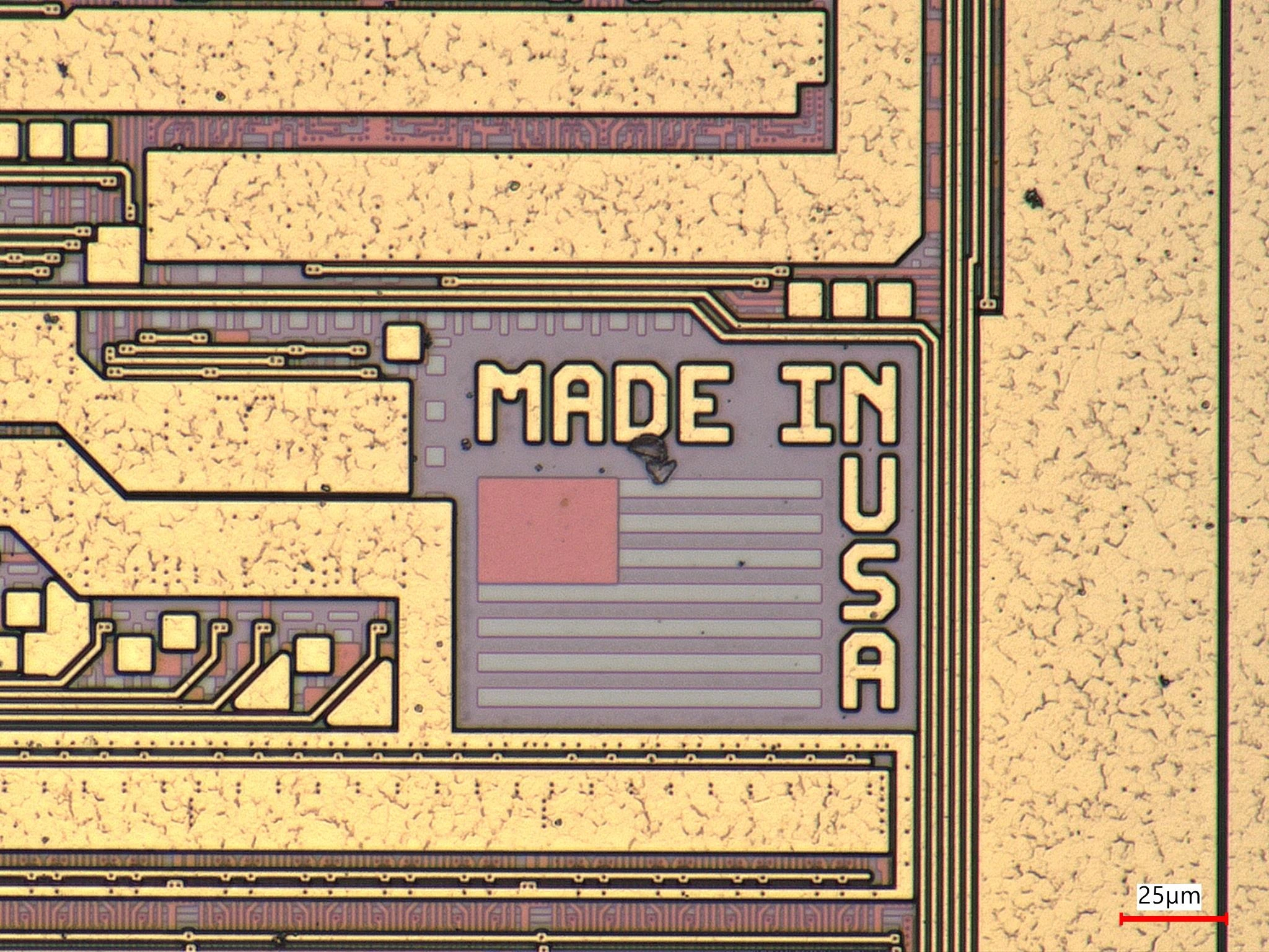
8. Component Decapsulation
To fully authenticate an electronic component, it is essential to inspect the semiconductor itself, as this provides highly revealing insights. To enable this, the encapsulating material is carefully removed, either chemically or thermally, exposing the die to light microscopy.
Once exposed, the semiconductor can be examined for its internal structures and markings. This method also enables the detection of possible defects, such as ESD damage. It is particularly effective for verifying authenticity and identifying signs of tampering or prior use.
All steps are standardized and documented in accordance with IDEA-STD-1010, AS6081, and AS6171.
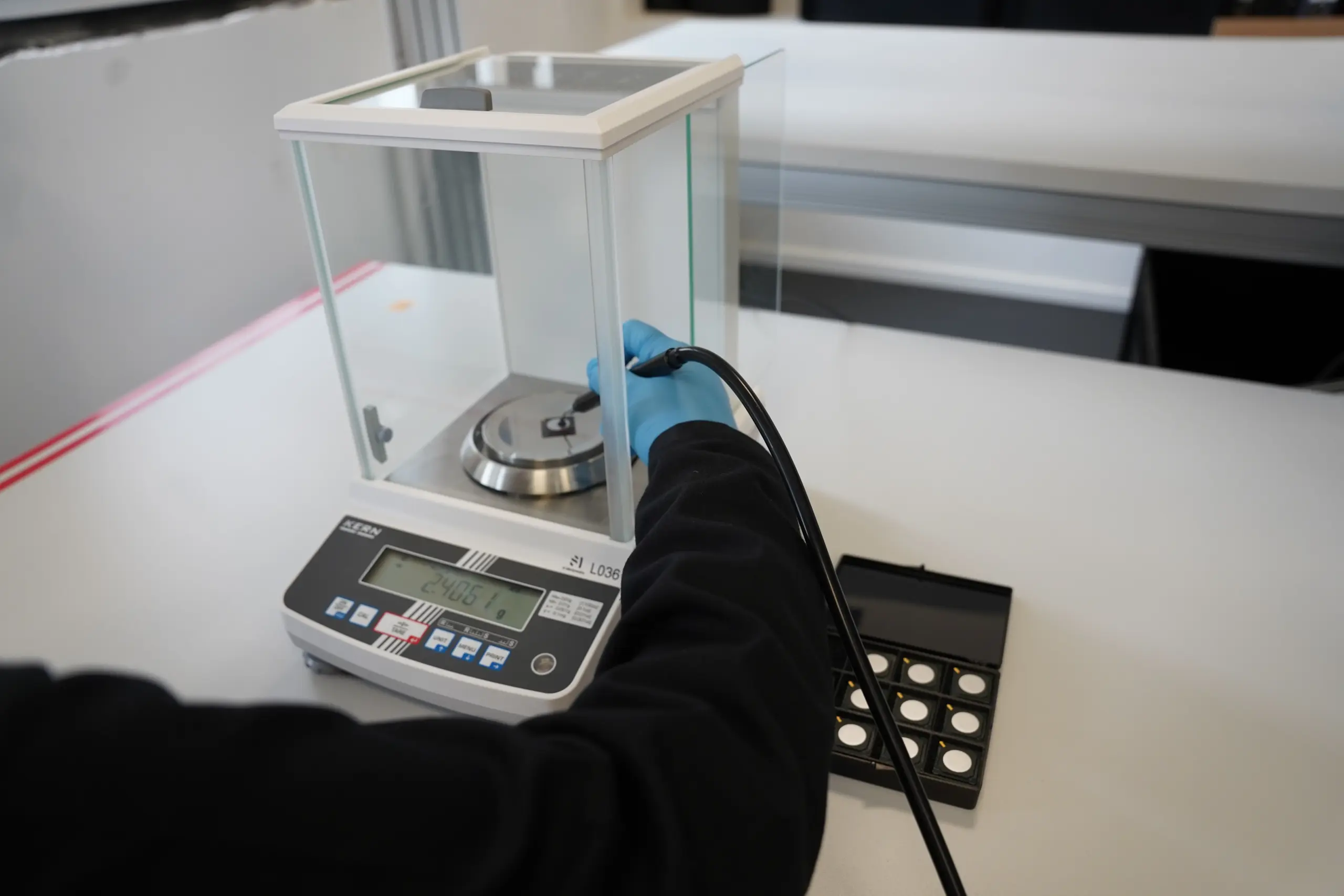
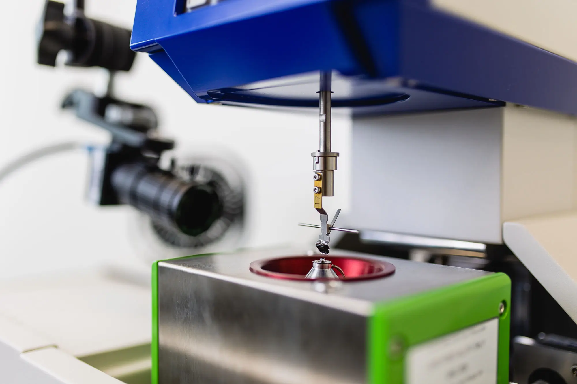
9. Solderability Testing
The processability of an electronic component is typically determined by its solderability. At the SI TechLAB, we use a wetting balance system to measure the wetting forces of solder contacts in the micronewton range to assess this property.
When combined with our other test methods, this approach enables a comprehensive evaluation of both the quality and processability of the components under investigation.

Traceable Test Results
Every test conducted at the SI TechLAB results in a clear, technically sound report. These reports feature high-resolution images, measurement data, and expert evaluations. They are standardized according to IDEA-STD-1010B, but can also be tailored to your needs. We provide the clarity you need to make confident decisions.
Do You Have Questions About a Specific Testing Requirement?
Talk to our team. We listen, ask the right questions, and deliver solutions that are both technically and logistically sound. Call us directly:
+49 621 405406-80